Comparison of Boron and Phosphorus Emitter Calculations by Griddler 2.5 Pro (v2.50021) cmd-PC1D-6.2 Caller to EDNA2 (v2.5.5) | 比较Griddler2.5 Pro(v2.50021) cmd-PC1D-6.2 Caller 和EDNA2 (v2.5.5)对硼和磷发射极的计算
Background | 背景
Griddler 2.5 PRO is equipped with a cell cross sectional diagram with an interface to cmd-PC1D-6.2 [1] for doped layer saturation current density J0e calculations, as well as internal quantum efficiency (IQE) calculations. cmd-PC1D-6.2 and PC1Dmod 6-2 are command line executed and graphic user interface versions of a fast, one-dimensional semiconductor device simulator written at the Institute for Energy Technology (IFE) Norway. It is open source and freely available for download. Another well known free calculator of silicon solar cell emitter J0e and IQE is EDNA2 [2], developed and hosted online by PV Lighthouse. The authors and collaborators of a previous version of cmd-PC1D-6.2 (v6.1) have compared the J0e calculations between cmd-PC1D-6.1 and EDNA2, for a variety of Gaussian shaped boron and phosphorus silicon emitter profiles, and found good agreement between the two calculators [3]. In this section, we will compare both J0e and IQE calculations between cmd-PC1D-6.2 and EDNA2 (v2.5.5), for a variety of boron and phosphorus silicon emitter profiles that we select from electrochemical capacitance voltage (ECV) measurements. Specifically, the cmd-PC1D-6.2 results are obtained by running the Griddler 2.5 PRO (v2.50021) interface, so the comparison is between the Griddler 2.5 PRO (v2.50021) cmd-PC1D-6.2 Caller and EDNA2 (v2.5.5).
Griddler 2.5 PRO 搭载了与cmd-PC1D-6.2 [1] 相链接的cell cross sectional diagram页面,用以计算掺杂层饱和复合电流密度J0e,以及内量子效率IQE。cmd-PC1D-6.2和PC1Dmod 6-2 是挪威能源技术研究所(IFE)编写的快速一维半导体器件模拟器中,以命令行执行的图形用户界面版本。 它是开源的并且可以免费下载。另一个广为人知的免费的硅太阳能电池J0e,IQE 计算器是PV Lighthouse开发并提供在线应用的EDNA2 [2]. 上一个版本的cmd-PC1D-6.2 (v6.1)的作者及其合作者,比较了用cmd-PC1D-6.1 和EDNA2计算高斯分布的硼和磷掺杂区J0e 的情况,并发现两者基本吻合[3]。这一小节,我们将会比较用 cmd-PC1D-6.2 和EDNA2 (v2.5.5)同时计算J0e 和IQE,并且计算中涉及的硼磷掺杂区掺杂曲线均为采用电化学电容-电压法测得的实际曲线。需要强调的是,cmd-PC1D-6.2 的计算结果是通过运行 Griddler 2.5 PRO (v2.50021)获得的。所以,我们实际比较的是Griddler 2.5 PRO (v2.50021) cmd-PC1D-6.2 Caller 和EDNA2 (v2.5.5).
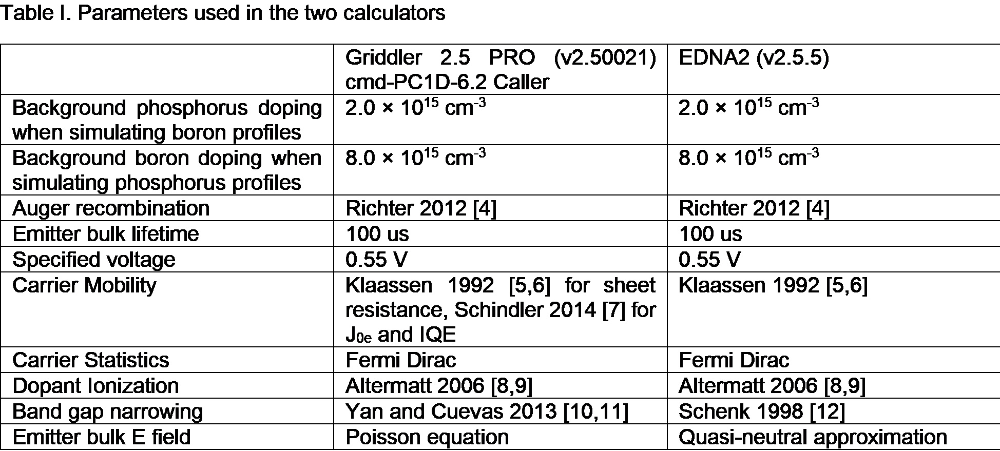
Table I compares the simulation parameters used by the two calculators. The two calculators have some differences in the modelling procedure. For example, EDNA2 assumes that the emitter is quasi-neutral, while cmd-PC1D-6.2 solves the electric field inside the emitter. The two calculators also use different methods to calculate bandgap narrowing. A variety of boron and phosphorus emitter profiles have been fed to both calculators. When simulating boron profiles, the phosphorus base doping of the cell is set to 2.0 × 10^15 cm^-3, and when simulating phosphorus profiles, the boron base doping of the cell is set to 8.0 × 10^15 cm^3. The bulk SRH lifetime of the emitter is always set to 100 us. The surface recombination velocity (SRV) for each case is set to different values and is recorded down in Tables II and III.
表1比较了两个模拟器中使用的参数。两个模拟器在模拟过程中稍稍有些区别。比如,EDNA2假设发射极是准中性的;但cmd-PC1D-6.2有计算发射极中的电场。这两个模拟器在计算带隙变窄效应方面也略有不同。
我们利用两个模拟器计算了许多不同硼和磷掺杂的情况。当计算硼掺杂区的情况时,磷的体掺杂浓度是 2.0 × 10^15 cm^-3。 当计算磷掺杂区的情况时,硼的体掺杂浓度是8.0 × 10^15 cm^3。 体SRH寿命一直都被设为100 us。每种情况的表面复合速度(SRV)都不尽相同,详情参见表2和表3。
Boron Emitter Calculations | 硼发射极计算
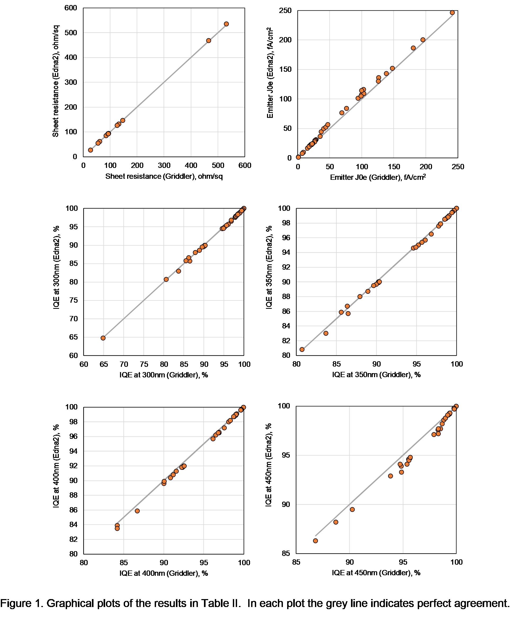
Figure 1 below compares the sheet resistance, J0e and IQE at the wavelengths 300, 350, 400, 450 nm, obtained by the two calculators, for a variety of different boron doping profiles and different surface recombination velocities. The agreement is generally very good. Average fractional deviations between the two calculators are 0.17%, 6.8%, 0.18%, 0.21%, 0.3%, 0.57%, for the sheet resistance, J0e, IQE300, IQE350, IQE400, IQE450, respectively. Therefore, the two calculators can be used interchangeably for boron emitters for practical intents.
图1比较了两个模拟器计算的薄层电阻,J0e 和波长为300, 350,400 和450 nm时的IQE。其结果吻合得很好。对于薄层电阻,J0e,IQE300,IQE350,IQE400,IQE450的计算,两个模拟器之间的平均分数偏差分别为0.17%, 6.8%,0.18%,0.21%,0.3%,0.57%。因此,在实际应用中的对硼发射极的计算,两个模拟器可以互换使用。
Phosphorus Emitter Calculations | 磷发射极计算
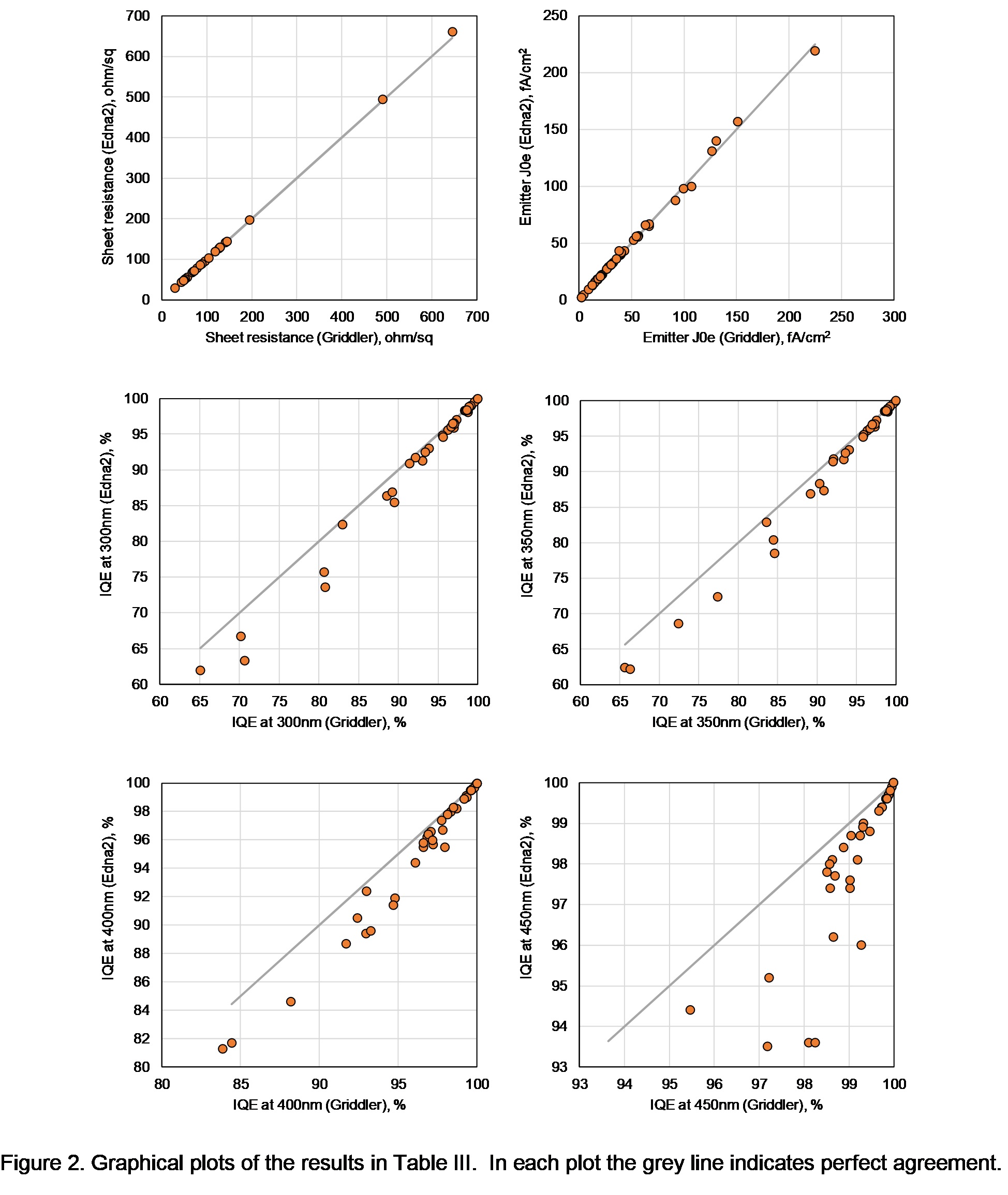
Figure 2 below compares the sheet resistance, J0e and IQE at the wavelengths 300, 350, 400, 450 nm, obtained by the two calculators, for a variety of different phosphorus doping profiles and different surface recombination velocities. The agreement is generally very good except for IQE. Average fractional deviations between the two calculators are 0.3%, 2.8%, 6.0%, 4.5%, 21%, 26% for the sheet resistance, J0e, IQE300, IQE350, IQE400, IQE450, respectively.
Therefore, the two calculators can be used interchangeably for phosphorus emitters sheet resistance and J0e calculations for practical intents. For IQE calculations the agreement is also good enough to yield very similar Jsc results.
图2比较了两个模拟器计算的薄层电阻,J0e 和波长为300, 350,400 和450 nm时的IQE。其结果吻合得很好。对于薄层电阻,J0e,IQE300,IQE350,IQE400,IQE450的计算,两个模拟器之间的平均分数偏差分别为0.3%, 2.8%, 6.0%, 4.5%, 21%, 26%。
因此,在实际应用中的对磷发射极的计算,两个模拟器可以互换使用。在计算的IQE方面,二者的吻合程度足以得出类似的Jsc结果。
References | 参考文献
[1] H. Haug, J. Greulich, “PC1Dmod 6.2 – Improved simulation of c-Si devices with updates on device physics and user interface”, Energy Procedia, vol 92, pp. 60-68, 2016.
[2] K.R. McIntosh and P.P. Altermatt, "A freeware 1D emitter model for silicon solar cells," 35th IEEE Photovoltaic Specialists Conference, Honolulu, pp. 2188–2193, 2010.
[3] H. Haug, A. Kimmerle, J. Greulich, A. Wolf, E. S. Marstein, “Implementation of Fermi–Dirac statistics and advanced models in PC1D for precise simulations of silicon solar cells”, Solar Energy Materials and Solar Cells, vol. 131, pp. 30-36, 2014.
[4] A. Richter, S. W. Glunz, F. Werner, J. Schmidt, and A. Cuevas, "Improved quantitative description of Auger recombination in crystalline silicon," Physical Review B, vol. 86, pp. 1-14, 2012.
[5] D. B. M. Klaassen, "A unified mobility model for device simulation - I. Model equations and concentration dependence," Solid-State Electronics, vol. 35, pp. 953-9, 1992.
[6] D. B. M. Klaassen, "A unified mobility model for device simulation - II. Temperature dependence of carrier mobility and lifetime. ," Solid State Electronics, vol. 35, pp. 961-7, 1992.
[7] F. Schindler, M. Forster, J. Broisch, J. Schön, J. Giesecke, S. Rein, et al., "Towards a unified low-field model for carrier mobilities in crystalline silicon," Solar Energy Materials and Solar Cells, vol. 131, pp. 92-99, 2014.
[8] P. P. Altermatt, A. Schenk, and G. Heiser, "A simulation model for the density of states and for incomplete ionization in crystalline silicon. I. Establishing the model in Si : P," Journal of Applied Physics, vol. 100, p. 113714, 2006.
[9] P. P. Altermatt, A. Schenk, B. Schmithusen, and G. Heiser, "A simulation model for the density of states and for incomplete ionization in crystalline silicon. II. Investigation of Si : As and Si : B and usage in device simulation," Journal of Applied Physics, vol. 100, p. 113715, Dec 1 2006.
[10] D. Yan and A. Cuevas, "Empirical determination of the energy band gap narrowing in highly doped n+ silicon," Journal of Applied Physics, vol. 114, p. 044508, 2013.
[11] D. Yan and A. Cuevas, "Empirical determination of the energy band gap narrowing in p+ silicon heavily doped with boron," Journal of Applied Physics, vol. 116, p. 194505, 2014.
[12] A. Schenk, "Finite-temperature full random-phase approximation model of band gap narrowing for silicon device simulation," Journal of Applied Physics, vol. 84, pp. 3684-95, 1998.