
Two Diode Network Model of a Solar Cell
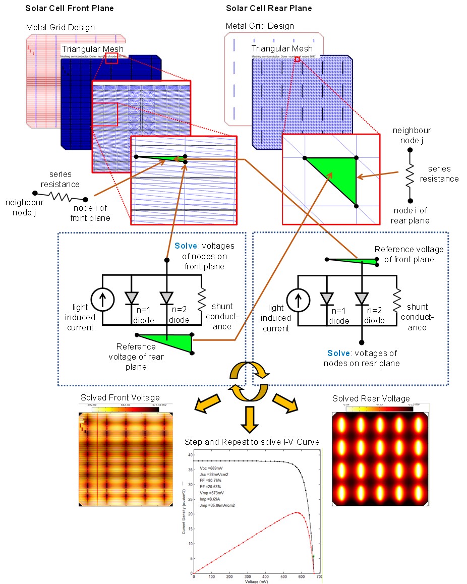
The core of Griddler is a finite element model (FEM) representation of the solar cell planes as shown above. Generally there can be 1 to 8 planes: simplest case being 1 plane to describe a simple grid on the front side, while the rear side is assumed to be perfectly laterally conductive and at ground potential; most complex case is that for each of the front and rear sides there are separately the semiconductor plane, metal finger plane (if there is contact resistance between the fingers and semiconductor), metal busbar plane (if the user chooses dual print to make the busbars “floating”), and ribbons plane (if the user chooses “Solder ribbons at probe points” under the Current Extraction option). In the FEM representation, these planes (except the ribbons planes) are finely broken down into triangular meshes to implement the network model of the solar cell. The above picture shows a triangle element on each of the meshed front and rear semiconductor planes in green. The corners of the triangles are called nodes and each node has a voltage. The edges of the triangles connect the nodes together via resistors whose values depend on the sheet resistance of the region (e.g. relatively high values for semiconductor, low values for metal fingers and busbars), as well as the triangle shape according to the Galerkin method.
Between the front and rear semiconductor planes is a sandwich layer where the photovoltaic properties of the solar cell are implemented. This sandwich layer provides a small equivalent circuit that connects to each node of the semiconductor layers, as shown inside the dotted blue boxes above. The equivalent circuit is also called the two diode model, because it is defined by two diodes of different I-V characteristics in describing the recombination currents happening inside the node. An additional current source is in parallel to these diodes to describe the light-induced current, and a parallel shunt conductance is used to describe shunt currents if any. The I-V characteristics of the equivalent circuit is:
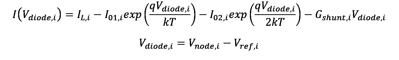
Where Vdiode,i is the voltage across the equivalent circuit, q is the elementary charge, k is the Boltzmann constant, T is the cell temperature in Kelvin. IL,i is the light induced current, I01,i and I02,i are the saturation currents of the n=1 and n=2 diodes, and Gshunt,i is the shunt conductance. Vdiode,i is given by Vnode,i – Vref,i, where Vnode,i is the voltage of the node i of concern, and Vref,i is an interpolated value of the voltage on the opposite semiconductor plane at the position of the node i. With this, we can formulate the current continuity condition at node i using Kirchhoff’s node law:
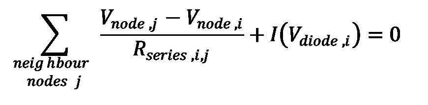
This allows a system of equations to be constructed for the voltages of the nodes to be solved iteratively. Once the semiconductor node voltages are solved on each plane, Vdiode,i and I(Vdiode,i) are also simultaneously determined. The overall current of the solar cell is then simply the sum of I(Vdiode,i) across all nodes on either the front or rear semiconductor planes, and the overall voltage of the solar cell is then the difference between the front node voltage where current is extracted, and the rear node voltage where current is extracted.
The operating point of the solar cell is defined by the level of illumination, as given by IL,i, and the terminal voltage which sets the boundary condition of the front nodes where current is extracted. The rear node voltage where current is extracted is usually set to zero (ground). By a step and repeat process where the terminal voltage is varied and then the cell voltage is solved, one forms the overall I-V characteristics of the solar cell.