Comparison of Boron and Phosphorus Emitter Calculations by Griddler 2.5 Pro (v2.50021) cmd-PC1D-6.2 Caller to EDNA2 (v2.5.5)
Background
Griddler 2.5 PRO is equipped with a cell cross sectional diagram with an interface to cmd-PC1D-6.2 [1] for doped layer saturation current density J0e calculations, as well as internal quantum efficiency (IQE) calculations. cmd-PC1D-6.2 and PC1Dmod 6-2 are command line executed and graphic user interface versions of a fast, one-dimensional semiconductor device simulator written at the Institute for Energy Technology (IFE) Norway. It is open source and freely available for download. Another well known free calculator of silicon solar cell emitter J0e and IQE is EDNA2 [2], developed and hosted online by PV Lighthouse. The authors and collaborators of a previous version of cmd-PC1D-6.2 (v6.1) have compared the J0e calculations between cmd-PC1D-6.1 and EDNA2, for a variety of Gaussian shaped boron and phosphorus silicon emitter profiles, and found good agreement between the two calculators [3]. In this section, we will compare both J0e and IQE calculations between cmd-PC1D-6.2 and EDNA2 (v2.5.5), for a variety of boron and phosphorus silicon emitter profiles that we select from electrochemical capacitance voltage (ECV) measurements. Specifically, the cmd-PC1D-6.2 results are obtained by running the Griddler 2.5 PRO (v2.50021) interface, so the comparison is between the Griddler 2.5 PRO (v2.50021) cmd-PC1D-6.2 Caller and EDNA2 (v2.5.5).
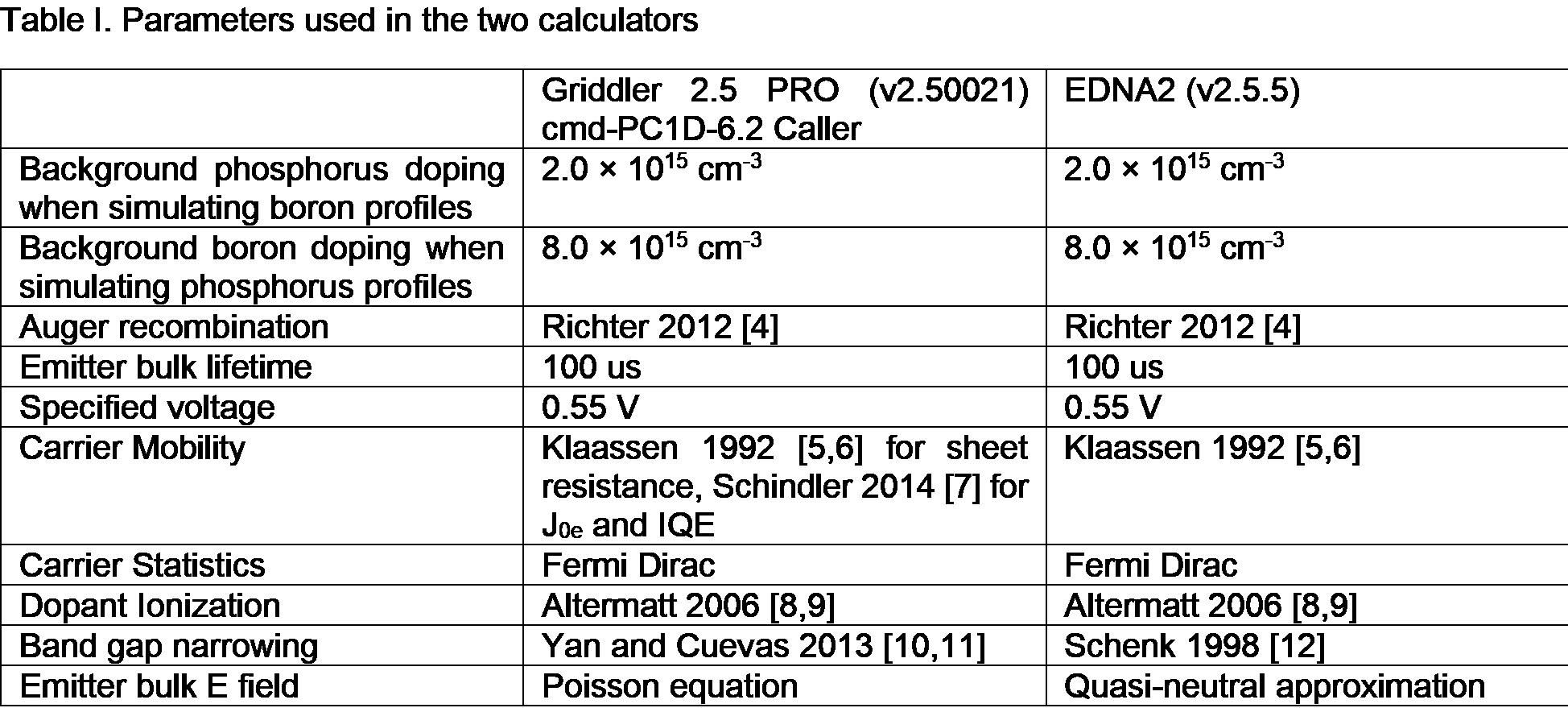
Table I compares the simulation parameters used by the two calculators. The two calculators have some differences in the modelling procedure. For example, EDNA2 assumes that the emitter is quasi-neutral, while cmd-PC1D-6.2 solves the electric field inside the emitter. The two calculators also use different methods to calculate bandgap narrowing. A variety of boron and phosphorus emitter profiles have been fed to both calculators. When simulating boron profiles, the phosphorus base doping of the cell is set to 2.0 × 10^15 cm^-3, and when simulating phosphorus profiles, the boron base doping of the cell is set to 8.0 × 10^15 cm^3. The bulk SRH lifetime of the emitter is always set to 100 us. The surface recombination velocity (SRV) for each case is set to different values and is recorded down in Tables II and III.
Boron Emitter Calculations
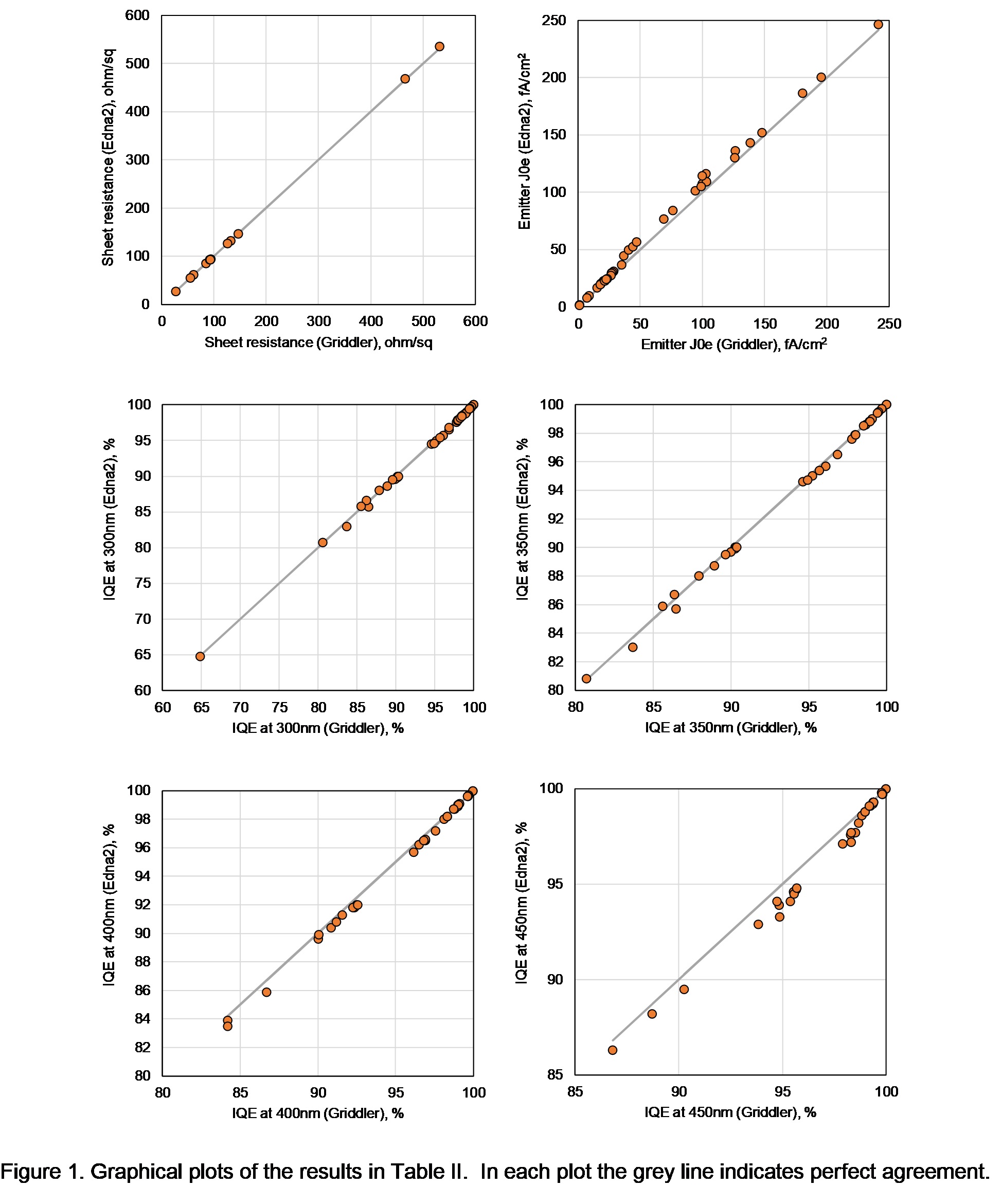
Figure 1 below compares the sheet resistance, J0e and IQE at the wavelengths 300, 350, 400, 450 nm, obtained by the two calculators, for a variety of different boron doping profiles and different surface recombination velocities. The agreement is generally very good. Average fractional deviations between the two calculators are 0.17%, 6.8%, 0.18%, 0.21%, 0.3%, 0.57%, for the sheet resistance, J0e, IQE300, IQE350, IQE400, IQE450, respectively. Therefore, the two calculators can be used interchangeably for boron emitters for practical intents.
Phosphorus Emitter Calculations
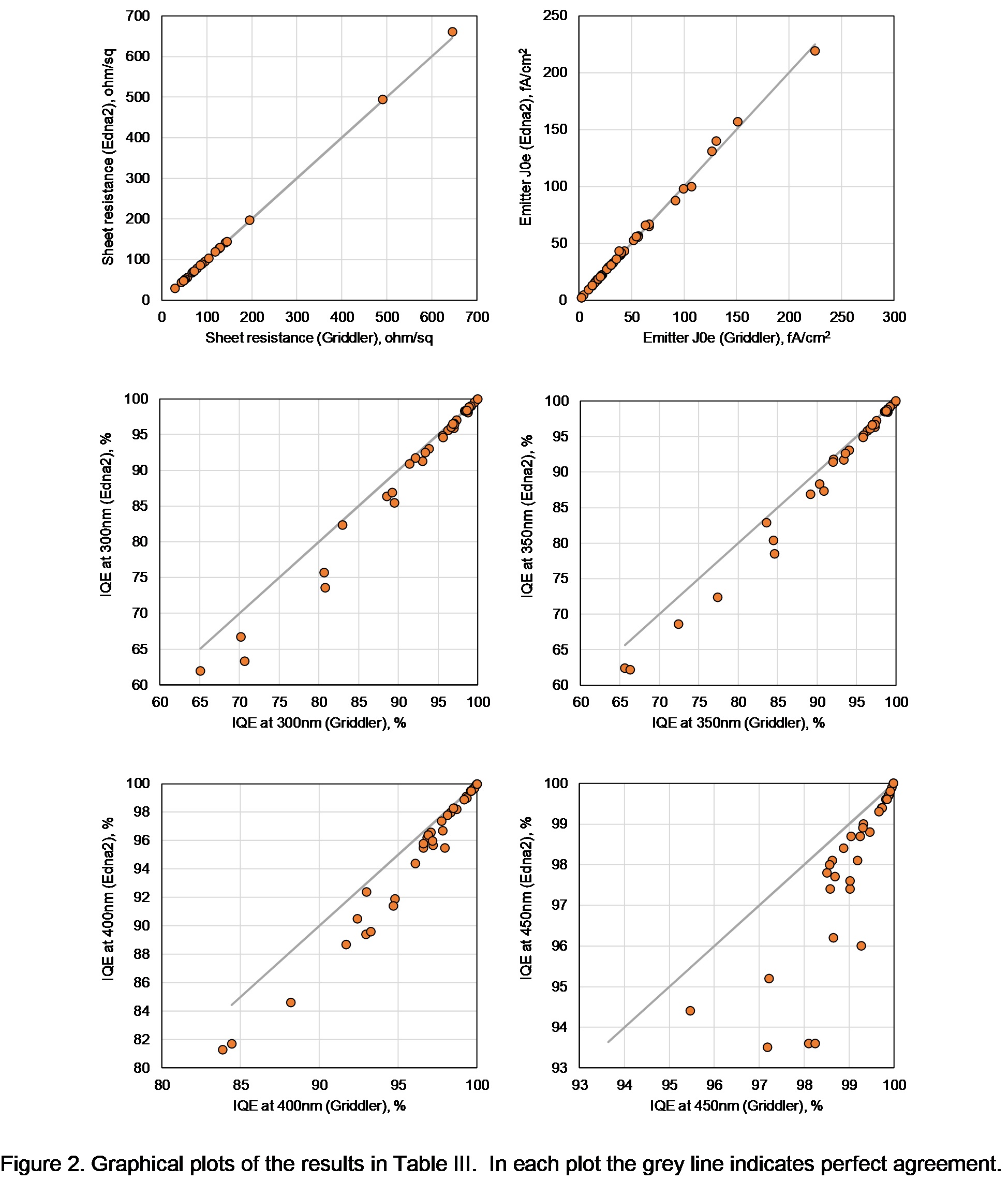
Figure 2 below compares the sheet resistance, J0e and IQE at the wavelengths 300, 350, 400, 450 nm, obtained by the two calculators, for a variety of different phosphorus doping profiles and different surface recombination velocities. The agreement is generally very good except for IQE. Average fractional deviations between the two calculators are 0.3%, 2.8%, 6.0%, 4.5%, 21%, 26% for the sheet resistance, J0e, IQE300, IQE350, IQE400, IQE450, respectively.
Therefore, the two calculators can be used interchangeably for phosphorus emitters sheet resistance and J0e calculations for practical intents. For IQE calculations the agreement is also good enough to yield very similar Jsc results.
References
[1] H. Haug, J. Greulich, “PC1Dmod 6.2 – Improved simulation of c-Si devices with updates on device physics and user interface”, Energy Procedia, vol 92, pp. 60-68, 2016.
[2] K.R. McIntosh and P.P. Altermatt, “A freeware 1D emitter model for silicon solar cells,” 35th IEEE Photovoltaic Specialists Conference, Honolulu, pp. 2188–2193, 2010.
[3] H. Haug, A. Kimmerle, J. Greulich, A. Wolf, E. S. Marstein, “Implementation of Fermi–Dirac statistics and advanced models in PC1D for precise simulations of silicon solar cells”, Solar Energy Materials and Solar Cells, vol. 131, pp. 30-36, 2014.
[4] A. Richter, S. W. Glunz, F. Werner, J. Schmidt, and A. Cuevas, “Improved quantitative description of Auger recombination in crystalline silicon,” Physical Review B, vol. 86, pp. 1-14, 2012.
[5] D. B. M. Klaassen, “A unified mobility model for device simulation – I. Model equations and concentration dependence,” Solid-State Electronics, vol. 35, pp. 953-9, 1992.
[6] D. B. M. Klaassen, “A unified mobility model for device simulation – II. Temperature dependence of carrier mobility and lifetime. ,” Solid State Electronics, vol. 35, pp. 961-7, 1992.
[7] F. Schindler, M. Forster, J. Broisch, J. Schön, J. Giesecke, S. Rein, et al., “Towards a unified low-field model for carrier mobilities in crystalline silicon,” Solar Energy Materials and Solar Cells, vol. 131, pp. 92-99, 2014.
[8] P. P. Altermatt, A. Schenk, and G. Heiser, “A simulation model for the density of states and for incomplete ionization in crystalline silicon. I. Establishing the model in Si : P,” Journal of Applied Physics, vol. 100, p. 113714, 2006.
[9] P. P. Altermatt, A. Schenk, B. Schmithusen, and G. Heiser, “A simulation model for the density of states and for incomplete ionization in crystalline silicon. II. Investigation of Si : As and Si : B and usage in device simulation,” Journal of Applied Physics, vol. 100, p. 113715, Dec 1 2006.
[10] D. Yan and A. Cuevas, “Empirical determination of the energy band gap narrowing in highly doped n+ silicon,” Journal of Applied Physics, vol. 114, p. 044508, 2013.
[11] D. Yan and A. Cuevas, “Empirical determination of the energy band gap narrowing in p+ silicon heavily doped with boron,” Journal of Applied Physics, vol. 116, p. 194505, 2014.
[12] A. Schenk, “Finite-temperature full random-phase approximation model of band gap narrowing for silicon device simulation,” Journal of Applied Physics, vol. 84, pp. 3684-95, 1998.